67 ~ VHDL Project : UART System Explained (VHDL) : UART HLD Block Diagram
2026-05-24
Channel: Learn And Grow Community (3230 subscribers)
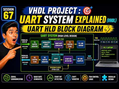
UART is one of those protocols that everyone uses but few people truly understand at the gate level. This video tackles the high-level design (HLD) block diagram of a UART system implemented in VHDL — the kind of structured approach you'd actually use in a real FPGA project rather than copy-pasting a transmitter module from a tutorial.
The value here is in the decomposition. A working UART isn't just a shift register; it's a baud rate generator, a transmitter FSM, a receiver FSM with oversampling for mid-bit sampling, FIFO buffers, and a parity/framing error detection layer. Walking through the HLD block diagram before touching code is exactly how senior FPGA engineers approach IP design, and it's a habit that separates hobbyists from professionals.
For anyone learning VHDL or preparing for VLSI interviews, understanding UART end-to-end is almost mandatory — it's the canonical "first real protocol" project and frequently shows up in coding rounds. The channel appears to be part of a numbered series (this is episode 67), so viewers who want to go deeper can follow along to the low-level implementation episodes that presumably follow.
Pair this with a Basys 3 or DE10-Lite board and you'll have a tangible project for your portfolio that demonstrates digital design fundamentals: clock domain awareness, FSM design, and serial protocol timing.
