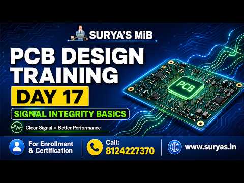
PCB Design Training Day 17 | Microcontroller PCB Design | Complete Embedded Hardware Layout
2026-05-18
Channel: SURYA'S MiB (54 subscribers)
Most of today's candidates are hashtag-stuffed shorts, capstone demo reels with no explanation, or background-music project clips. This one stands out because it's part of a structured, day-by-day PCB design training series — Day 17 specifically tackles laying out a complete microcontroller-based board.
Microcontroller PCB layout is one of those topics where the gap between "I can route a blinky LED" and "my board actually works at 50 MHz without resetting itself" is enormous. A proper walkthrough should cover decoupling capacitor placement near every VCC pin, crystal oscillator layout with guard traces and short return paths, reset circuitry, programming/debug header placement, and how to plan a sensible ground pour so high-speed signals have a clean return path.
Series-format channels like this one tend to be more pedagogical than one-off project videos because the creator has to think about progression — by Day 17, viewers presumably already know the schematic capture, footprint, and basic routing fundamentals, so the instructor can focus on the decisions rather than the mechanics. That's where the real learning lives.
At 54 subscribers this is a tiny channel, so quality is uncertain, but the topic and format are exactly what someone building their first non-trivial embedded board needs.
